Material Evolution File
Graphene From Graphite to Devices
Trace how a graphite layer became an isolated carbon material, then a test bed for electronics, coatings, sensors and composites.
Carbon source
Graphite Already Contained the Sheet
Selected file: Graphite Already Contained the Sheet. Choose another file to update this evidence card.
Layered structure
Graphite is made from stacked sheets of carbon atoms arranged in a hexagonal pattern. Weak attraction between the sheets lets graphite leave marks on paper and also made separation imaginable.
Not yet graphene
A graphite crystal is three-dimensional. Graphene refers to a single atomic layer, where electrons, surface area and mechanical behavior are no longer averaged across many stacked layers.
Early obstacle
Scientists could describe isolated carbon layers in theory, yet handling a stable sheet one atom thick under ordinary laboratory conditions remained doubtful before the 2000s.
Graphene was not invented from a new element; it was separated from a familiar carbon solid in a new physical form.
2D material idea
The One-Atom Lattice Became a Target
Selected file: The One-Atom Lattice Became a Target. Choose another file to update this evidence card.
Flat carbon network
The ideal graphene sheet is a two-dimensional honeycomb lattice. Each carbon atom bonds to three neighbors, leaving electronic states that give graphene unusual charge behavior.
Stability question
Thermal motion and surface contamination were expected to make free, perfect two-dimensional crystals hard to preserve. The lab challenge was not naming the sheet but isolating and measuring it.
Carbon relatives
Fullerenes and carbon nanotubes showed that carbon could form nanoscale structures. Graphene supplied the flat reference layer from which nanotubes can be viewed as rolled sheets.
The theoretical sheet gave researchers a clear object to seek, but proof required a measurable, isolated layer.
Isolation record
Mechanical Exfoliation Made It Visible
Selected file: Mechanical Exfoliation Made It Visible. Choose another file to update this evidence card.
Manchester work
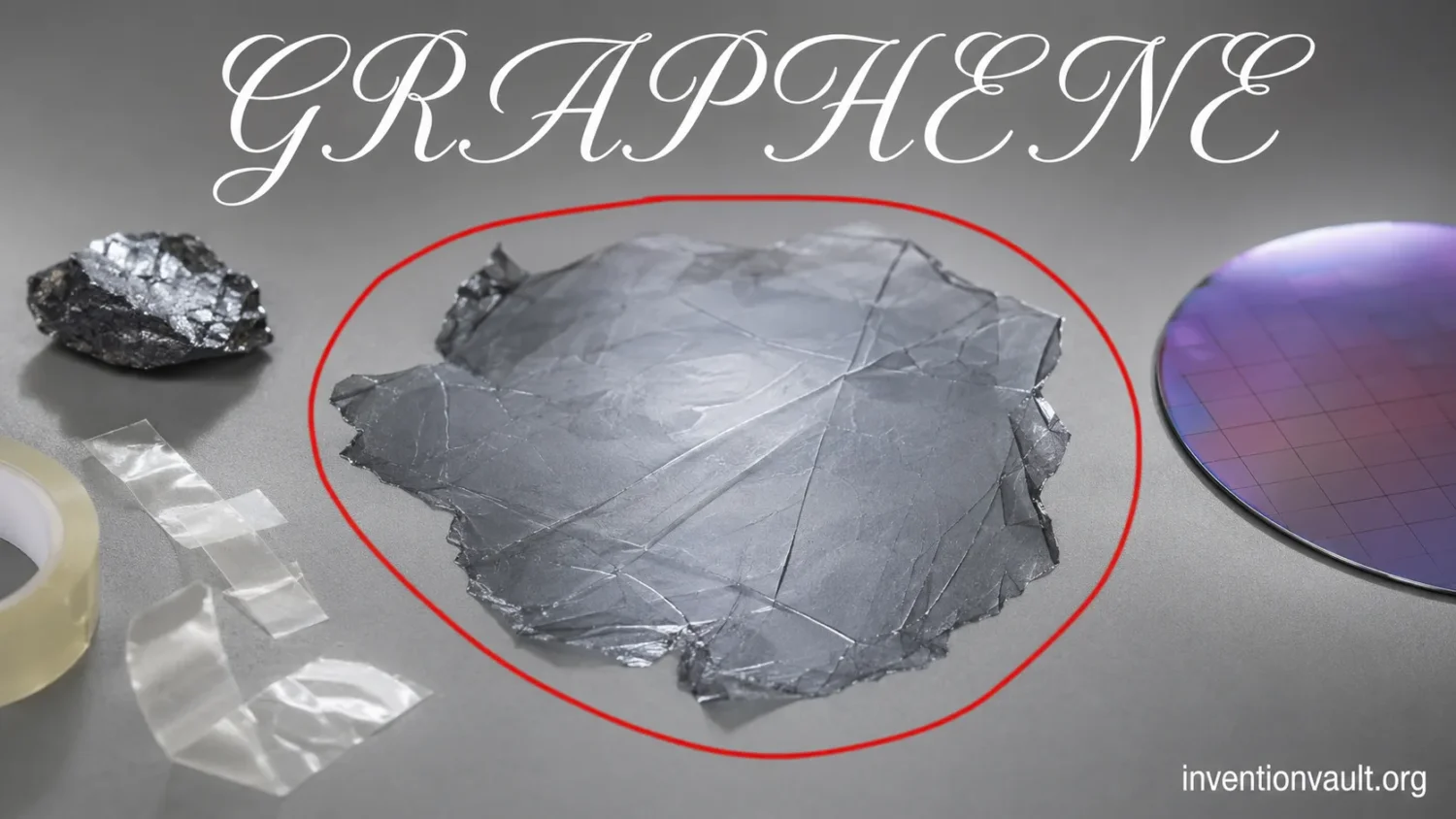
In 2004, Andre Geim, Konstantin Novoselov and co-workers reported atomically thin carbon films made by peeling graphite and transferring flakes to a substrate.
Optical detection
Silicon dioxide on silicon made thin flakes visible under an optical microscope through contrast effects, allowing researchers to find and contact suitable pieces.
Research-grade sheets
The peeled flakes were small, but they were clean enough for electrical measurements. That mattered more than size for proving the material’s behavior.
The tape method did not create factory graphene, but it supplied the clean specimens that made the material measurable.
Electronic behavior
Gate Voltage Revealed Tunable Carriers
Selected file: Gate Voltage Revealed Tunable Carriers. Choose another file to update this evidence card.
Field effect
The 2004 paper showed that applying voltage could shift the balance between electron and hole carriers. That made graphene a controllable conducting channel rather than only a curiosity.
Room-temperature motion
Early flakes showed high carrier mobility at room temperature compared with many thin films. That drew attention from electronics researchers looking beyond conventional transistor channels.
Band-gap limit
Graphene conducts too readily for many digital switching roles unless its electronic structure is altered. This is why it has not simply replaced silicon logic.
Graphene’s electrical promise came with a constraint: excellent conduction is not the same as easy transistor switching.
Production route
Growth Methods Moved Beyond Flakes
Selected file: Growth Methods Moved Beyond Flakes. Choose another file to update this evidence card.
Copper foils
Chemical vapor deposition on metals, especially copper, gave researchers a way to grow larger graphene films, then transfer them to other surfaces.
Trade-offs
Large area does not automatically mean perfect material. Grain boundaries, wrinkles, residue and transfer damage can change conductivity, strength and device yield.
Powder forms
Graphene nanoplatelets and graphene oxide can be made in bulk for inks, coatings and composites, but these are not always single-layer, defect-free graphene.
Scale changed graphene from a laboratory flake into a family of manufactured carbon materials with varied quality levels.
Applied forms
Applications Followed the Form Available
Selected file: Applications Followed the Form Available. Choose another file to update this evidence card.
Transparent conductors
Large thin films are studied for transparent electrodes and flexible electronics, where optical transparency and conductivity must be balanced against cost and uniformity.
Composite additives
Small amounts of graphene-derived material can alter stiffness, electrical pathways or barrier performance in polymers and coatings, provided dispersion and bonding are controlled.
Metrology and standards
Reliable use depends on measurement: layer count, defect density, oxygen content, flake size and contamination can decide whether two “graphene” samples behave alike.
Graphene’s legacy is not one product; it is a material platform whose value depends on form, quality and measurement.
Graphene is a single layer of carbon atoms arranged in a hexagonal lattice. It was not invented like a machine with a patentable assembly; it was isolated, measured and then developed into manufacturable forms. The usual historical turning point is the 2004 work by Andre Geim, Konstantin Novoselov and colleagues at the University of Manchester, who separated atomically thin carbon flakes from graphite and demonstrated their unusual electronic behavior.
| Item | Graphene detail |
|---|---|
| Material class | Two-dimensional carbon material |
| Atomic structure | One-atom-thick sheet of carbon atoms in a honeycomb lattice |
| Source material | Graphite, the layered form of carbon used in pencils and electrodes |
| Modern discovery milestone | 2004 isolation and electrical measurement of atomically thin carbon films |
| Nobel recognition | 2010 Nobel Prize in Physics to Andre Geim and Konstantin Novoselov |
| Main production routes | Mechanical exfoliation, chemical vapor deposition, epitaxial growth, liquid-phase exfoliation and oxidation-reduction routes |
What Graphene Is
Graphene is the one-layer form of graphite. In graphite, many graphene-like sheets are stacked together. Each sheet is made from carbon atoms joined to three neighbors, forming a flat pattern of hexagons. When one sheet is separated from the stack, its electrons and surface behavior are no longer hidden inside a bulk crystal.
This one-layer geometry gives graphene several properties that drew attention after 2004: high electrical conductivity, high carrier mobility in clean samples, high in-plane strength, flexibility, optical transparency in thin films and a very large surface area per mass. These traits do not appear equally in every commercial graphene product. They depend on layer count, flake size, defects, oxygen content, substrate and processing route.
Discovery or Invention?
Graphene is best described as a discovered and engineered material. Carbon sheets existed inside graphite; the breakthrough was isolating, identifying and measuring a stable one-atom-thick form, then developing methods to make useful quantities.
Before Graphene: Graphite, Carbon Nanotubes and the 2D Problem
Graphite had been familiar for centuries as a layered carbon solid. Its layers explain why it is soft, slippery and able to leave a dark trace on paper. The same weak attraction between layers suggested that very thin sheets might be separated, but a single atomic sheet was expected to be hard to preserve and handle.
Carbon research had already moved into nanoscale forms before graphene’s modern discovery. Fullerenes showed that carbon could form closed cages, while carbon nanotubes showed that rolled carbon sheets could conduct electricity and possess high strength. Graphene completed the picture by making the flat sheet itself accessible for measurement.
The challenge was practical. A one-atom layer cannot be picked up like foil. It must be found on a substrate, contacted with electrodes, and distinguished from thicker flakes without destroying it. The Manchester group’s method solved enough of that problem to allow reliable experiments.
The 2004 Isolation by Mechanical Exfoliation
The best-known method used adhesive tape to peel thin layers from graphite. Repeated peeling produced flakes of varying thickness. These flakes were transferred onto silicon wafers coated with silicon dioxide, where optical contrast helped researchers identify very thin regions under a microscope.
The technique was simple in appearance but demanding in execution. The researchers had to locate suitable flakes, confirm their thickness, make electrical contacts, and test whether the carbon films remained continuous and conductive. The resulting 2004 paper reported atomically thin carbon films and showed that their charge carriers could be controlled by an electric field.
Dating the First
The 2004 date refers to isolated, measured atomically thin carbon films that launched modern graphene research. It does not mean carbon layers were unknown before then, nor that large commercial films existed at that time.
How Graphene Works as an Electronic Material
Graphene’s electrical behavior comes from its lattice. The carbon atoms form a repeating pattern that allows electrons to move through the sheet in a way often described using relativistic-like physics. In simple terms, clean graphene can carry charge very efficiently across short distances.
The 2004 experiments used a gate voltage to change the carrier type and density in graphene. With the right voltage, the sheet could be shifted between electron-dominated and hole-dominated conduction. This field-effect behavior made graphene relevant to transistor research, even though graphene has a major limitation for ordinary digital logic: it has no natural band gap.
Graphene as a conductor
Graphene can conduct charge very well in clean, controlled conditions, and this makes it useful for research into sensors, electrodes, high-frequency devices and metrology.
Graphene as a logic switch
Digital transistors need a strong off state. Because pristine graphene lacks a natural band gap, it cannot simply take the place of silicon in standard logic chips.
From Laboratory Flakes to Larger Graphene Films
Mechanical exfoliation is excellent for producing small, clean flakes for research, but it is not a factory route for square meters of material. Scaling graphene required other methods. Chemical vapor deposition, often called CVD, became one of the main routes for growing graphene films on metal surfaces such as copper.
In a CVD process, carbon-containing gas decomposes on a heated metal surface, and carbon atoms assemble into a thin film. After growth, the graphene can be transferred to another substrate. This route opened work on transparent conductors, flexible electronics and wafer-scale experiments, but the transfer step can introduce wrinkles, tears and residues.
- Prepare the metalA metal surface such as copper is cleaned and heated so carbon atoms can arrange across it during growth.
- Introduce carbon gasA carbon-containing gas decomposes near the hot surface, supplying atoms that form a graphene layer.
- Control growthTemperature, gas flow and time influence layer count, grain size and continuity across the film.
- Transfer the sheetThe film is moved from the metal to a target substrate, a step that can add defects or contamination.
- Measure qualityRaman spectroscopy, microscopy and electrical tests help judge whether the film matches the intended use.
Graphene Oxide, Nanoplatelets and Commercial Material Names
Many products described as graphene are not pristine single-layer graphene. Graphene oxide contains oxygen-bearing groups that make it easier to disperse in water and process into films, papers or composites. Reduced graphene oxide removes some of that oxygen, improving conductivity but leaving defects and chemical changes.
Graphene nanoplatelets are small stacks or flakes containing one or more graphene layers. They are easier to make in larger volumes than perfect monolayers and are often used as additives in polymers, coatings, inks and thermal interface materials. Their value depends less on an ideal one-atom sheet and more on dispersion, particle shape, loading level and interaction with the host material.
Material Name
The word “graphene” can refer to pristine monolayer sheets, few-layer flakes, graphene oxide, reduced graphene oxide or nanoplatelets. These forms differ in conductivity, chemistry, strength and processability.
Why Graphene Became Scientifically Useful
Graphene became a favored research material because it links several properties in a single sheet. It can be thin and transparent, yet conductive. It can be flexible, yet strong along the plane of the carbon bonds. It exposes nearly all of its atoms to the surface, making it sensitive to nearby molecules, strain and electrical fields.
Those properties made graphene useful in physics labs first. It allowed researchers to study two-dimensional electron behavior, quantum Hall effects, charge transport, mechanical membranes and surface chemistry in a material that could be placed on a chip and contacted with electrodes.
Its later engineering appeal came from the same features. A coating may use graphene-derived flakes to reduce gas permeation. A polymer composite may use them to form conductive pathways. A sensor may exploit changes in graphene’s electrical response when molecules interact with its surface. A transparent electrode may use large-area graphene film where flexibility matters more than the very lowest resistance.
Applications and Their Limits
Graphene research has touched electronics, energy storage, membranes, coatings, biomedical interfaces, sensors, composites and quantum electrical standards. The path from laboratory result to product is uneven because each use needs a different material form. A sensor may tolerate small flakes. A display electrode needs a continuous, transparent, low-resistance film. A structural composite needs dispersion and bonding more than a perfect monolayer.
Cost is only one barrier. Quality control is often harder. Two batches with the same marketing name can differ in layer number, lateral size, defect density, oxygen content and contamination. These differences can change how the material disperses, conducts heat or electricity, bonds to polymers, or interacts with biological systems.
For this reason, graphene’s practical history is not a single race to replace another material. It is a gradual sorting process: matching each graphene form to a job where its thinness, surface area, conductivity, barrier behavior or mechanical response solves a defined problem.
Common Misunderstandings About Graphene
One misunderstanding is that graphene is always one perfect atomic layer. In research papers, the term may be tightly defined; in commercial materials, it may cover few-layer flakes or graphene-derived powders. Reading the material description matters.
A second misunderstanding is that graphene should have replaced silicon by now. Graphene is a superb conductor in many conditions, but digital logic needs controlled switching between on and off states. Pristine graphene’s lack of a natural band gap makes that task difficult without added engineering that can reduce some of the properties that made it attractive.
A third misunderstanding is that the adhesive-tape method was only a lucky trick. It was simple, but the research advance came from combining exfoliation, substrate choice, optical identification, microfabrication and electrical testing into a reliable experiment.
What Graphene Added to Material History
Graphene changed how researchers thought about two-dimensional materials. After graphene, many other atomically thin materials received renewed attention, including boron nitride, molybdenum disulfide and layered magnetic or superconducting materials. The deeper shift was not the arrival of one miracle material; it was the proof that a one-layer crystal could be isolated, contacted, measured and engineered.
Its history also shows a useful distinction between discovery and adoption. The 2004 work made graphene experimentally real. The 2010 Nobel Prize recognized that achievement. Manufacturing methods then turned graphene into films, powders, inks and composites with different levels of order and performance. Modern graphene remains both a research platform and an applied material family, with success depending on measurement and fit for purpose.
Questions People Ask About Graphene
Who discovered graphene?
Andre Geim, Konstantin Novoselov and their colleagues are credited with the 2004 experimental isolation and measurement that launched modern graphene research. Geim and Novoselov received the 2010 Nobel Prize in Physics for this work.
Is graphene stronger than steel?
Single-layer graphene has extremely high in-plane strength in ideal tests, but that does not mean a graphene product automatically outperforms steel. Bulk parts depend on defects, size, bonding, processing and the material system around the graphene.
Why is graphene not used everywhere?
Graphene must be made in the right form, at the right quality and cost, for each application. Transfer damage, defects, dispersion problems, lack of a natural band gap and inconsistent material naming have slowed some uses.
Is graphene the same as graphite?
No. Graphite is made from many stacked carbon layers. Graphene is one layer, or in some commercial contexts a small number of layers, separated from that stack or grown as a thin film.
References Used for This Article
- NIST Graphene program page — used for current scientific context on graphene’s electronic behavior and measurement-focused research.
- Nobel Prize, 2010 Physics press release — used for the Nobel recognition of Andre Geim and Konstantin Novoselov and the one-atom-thick carbon description.
- Novoselov et al., “Electric Field Effect in Atomically Thin Carbon Films,” Science, 2004 — used for the 2004 experimental report, field-effect behavior and room-temperature carrier mobility context.
- University of Manchester, Discovery of Graphene — used for the Manchester research setting and the mechanical exfoliation account.
- Li et al., “Large-Area Synthesis of High-Quality and Uniform Graphene Films on Copper Foils,” Science, 2009 — used for large-area chemical vapor deposition on copper foils.
- Graphene Flagship, Graphene material overview — used for applied material forms, properties and distinctions among graphene-related materials.