| Invention Name | Integrated Circuit (IC), often called a microchip |
| What It Is | A complete electronic circuit built on a single semiconductor die (usually silicon) |
| Core Breakthrough | Putting transistors, passive parts, and interconnect together so the “wiring” is made in the same process |
| Key Inventors | Jack S. Kilby (first working monolithic IC) and Robert N. Noyce (planar silicon IC concept); Jean A. Hoerni (planar process foundation) |
| First Working Demo | September 12, 1958 (Kilby’s germanium “solid circuit” demonstration) |
| From Prototype To Mass Production | The planar process and deposited metal interconnects made ICs practical for large-scale manufacturing |
| Early Commercial Families | 1961: Fairchild’s Micrologic series; October 1961: Texas Instruments announced planar “fully-integrated” logic family |
| Key Device Era Shift | MOS technology enabled very high density; CMOS made low-standby-power logic the default path |
| Why It Matters | It turned electronics into a scalable manufacturing problem, not a hand-wired assembly problem—unlocking small, reliable, and affordable systems |
| Common IC Categories | Digital, analog, mixed-signal, memory, power, RF, and SoC (system-on-chip) |
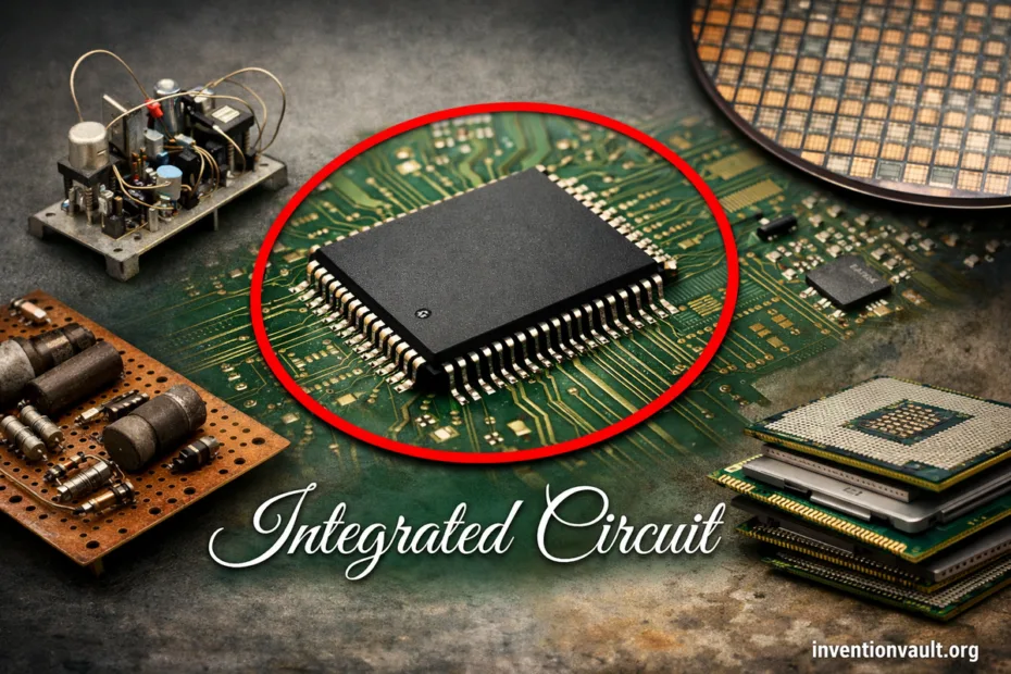
| What You Can See | A package with pins/contacts; inside is the die, bonding, and protective materials |
| Practical Note | Many ICs are ESD-sensitive; static electricity can harm tiny gate oxides |
Integrated circuits made electronics feel inevitable: once circuits could be built on silicon, the hard part shifted to design and manufacturing scale. Instead of thousands of separate parts and fragile wiring, an IC delivers a carefully controlled network of devices and interconnect layers in a footprint that can be smaller than a fingernail.
- Core Idea and Why It Matters
- What an Integrated Circuit Is
- What Is Built on the Die
- What the Package Adds
- How an IC Fits Inside a Package
- How Integrated Circuits Are Built
- Why the Planar Approach Was a Turning Point
- Main Types of ICs
- Integration Levels and What They Enabled
- Key Milestones
- Reading an IC Without Guesswork
- Datasheets Explain the Safe Operating Space
- Reliability and Handling Notes
- Where Integrated Circuits Show Up
- Common Terms
- References Used for This Article
Core Idea and Why It Matters
The big idea is simple: build many circuit elements on one semiconductor surface, then connect them with patterned metal so the circuit is “wired” by fabrication, not by hand. That is why an IC can be copied millions of times with consistent behavior and reliability.
- Size: functions that once needed a board can fit into a single package.
- Speed: short on-chip paths reduce delay and improve signal integrity.
- Cost: mass production makes each function cheaper when volume is high.
- Reliability: fewer external joints means fewer failure points.
What an Integrated Circuit Is
An integrated circuit is a completed set of electronic functions formed on a die—a tiny piece of semiconductor cut from a wafer. The die holds active devices (mostly transistors) plus supporting structures that guide currents and voltages with precision.
What Is Built on the Die
- Transistors that switch or amplify signals (MOSFETs dominate modern logic).
- Resistors and capacitors formed with semiconductor and thin-film structures.
- Diodes and protection devices for robust inputs.
- Metal interconnect layers separated by insulators to route signals.
- Passivation to shield sensitive surfaces from contamination.
What the Package Adds
- A safe way to connect the microscopic die to the macroscopic world.
- Mechanical protection for the fragile chip.
- Thermal paths to move heat away for stable operation.
- Standard shapes for assembly on PCBs with repeatable results.
How an IC Fits Inside a Package
When you hold an IC, you are holding its package, not the chip itself. Inside, the die is attached to a support, then connected to external pins by bond wires or flip-chip bumps. This hidden structure explains why packages vary so widely in shape and pin count.
| Package Style | What It Looks Like | Where It Fits Best |
|---|---|---|
| DIP (Dual In-Line) | Two rows of through-hole pins | Prototyping, education, legacy boards; easy handling |
| SOIC | Small surface-mount, gull-wing leads | General-purpose products where cost and density matter |
| QFN | No visible leads; pads under the body | Compact designs with good thermal performance |
| BGA | Solder balls in a grid under the chip | High pin counts; processors and SoCs |
| WLCSP | Wafer-level package, extremely small | Phones and wearables where space is tight |
How Integrated Circuits Are Built
IC fabrication is a layer-by-layer craft. Instead of carving a circuit from one block, manufacturers build thin films, patterns, and device regions in a repeated sequence. The exact recipes are tightly guarded, yet the big steps follow a shared logic that keeps modern production predictable.
- Wafer preparation: a polished silicon wafer becomes the base surface.
- Oxide and films: insulating and functional layers are grown or deposited with precision.
- Patterning: photolithography defines where materials stay or go using masks.
- Etching: selected areas are removed to form features and openings for later steps.
- Doping: controlled impurities create p/n regions, enabling transistor action.
- Metallization: metal layers form interconnects that route signals and power.
- Passivation: a protective top coat guards the finished surface from moisture and particles.
- Test and dicing: wafers are electrically tested, then cut into individual dies.
- Packaging: each die is attached, connected, sealed, and tested again for quality.
Why the Planar Approach Was a Turning Point
The planar approach created a flat, protected surface and made it practical to add metal “wiring” directly on the wafer. That single shift improved yield, raised reliability, and made large-scale integration realistic across many chip types.
Main Types of ICs
“Integrated circuit” describes the form, not one single function. ICs range from tiny analog helpers to systems-on-chip with processors, memory, and interfaces. Knowing the major families makes it easier to understand what an IC is designed to do and why its layout looks the way it does.
Analog ICs
Analog ICs shape continuous signals—voltage and current that move smoothly. Classic examples include op-amps, voltage references, and sensor front ends. Their design priorities focus on noise, stability, and predictable behavior across temperature.
Digital ICs
Digital ICs operate with discrete states—logic 0 and 1—built from logic gates and storage elements. They include microcontrollers, processors, and interface logic. The headline goals are speed, density, and low error under real-world electrical conditions.
Mixed-Signal ICs
Mixed-signal chips bridge analog and digital worlds in one package. ADCs and DACs are prime examples, along with audio codecs and many wireless chip blocks. Engineers work hard here because switching noise and precision must coexist on the same die.
Memory ICs
Memory chips store information as bits, whether for rapid access (SRAM, DRAM) or persistent storage (Flash, EEPROM). Their layouts repeat regular patterns, and their value comes from capacity and reliability over countless read/write cycles.
Power ICs
Power ICs manage energy: converting, regulating, and protecting supply rails. Think switch-mode regulators, charge controllers, and motor drivers. They are defined by efficiency, heat handling, and safe protection features that keep systems steady under load.
RF and High-Frequency ICs
RF ICs work where signals oscillate rapidly and layout becomes part of the circuit. Low-noise amplifiers, PLLs, and transceiver blocks live here. Designers prioritize matching, parasitics, and signal integrity so devices communicate cleanly.
Integration Levels and What They Enabled
Integration is the quiet force behind modern electronics. As feature sizes shrank and manufacturing matured, chips moved from a few gates to full computers on a die. That steady climb shaped products, markets, and even what people expect from everyday tehcnology in their pockets and homes.
| Integration Term | Typical Complexity | Common Examples |
|---|---|---|
| SSI | Dozens of devices; simple building blocks | Logic gates, basic flip-flops, small analog helpers |
| MSI | Hundreds of devices; functional blocks | Counters, multiplexers, small decoders |
| LSI | Thousands to tens of thousands of devices | Early memory, complex controllers, calculator and interface chips |
| VLSI | Millions and beyond; systems on a chip | Microprocessors, SoCs, dense memory |
Complexity Trend (Conceptual)
SSI   |■■
MSI   |■■■■
LSI   |■■■■■■■■
VLSI  |■■■■■■■■■■■■■■■■
Key Milestones
The integrated circuit has a clear timeline because a few technical leaps changed what was buildable and what was manufacturable. The dates below focus on widely recognized steps that shaped the mainstream IC era and the rise of modern electronics.
- September 12, 1958: first working monolithic IC demo by Jack S. Kilby.
- 1959: the planar process is introduced and the planar IC concept is advanced for scalable manufacturing.
- 1960: first planar integrated circuit fabrication milestones appear, proving the approach can work on silicon.
- 1961: early commercial IC families emerge, including Fairchild’s Micrologic series and TI’s planar logic announcements.
- 1963: CMOS circuit configuration is demonstrated as a low-standby-power logic path.
- 1964: first commercial MOS integrated circuits are introduced, pointing toward very dense chips.
- April 19, 1965: the famous “more components per chip” prediction is published, shaping expectations for scaling.
- November 15, 1971: Intel releases the 4004, a landmark single-chip CPU in a 16-pin DIP package.
Reading an IC Without Guesswork
Most chips tell you more than people expect—if you know what to look for. Markings vary by maker and era, yet the same signals appear again and again: identity, orientation, and traceability. This is especially helpful when you meet an IC outside its original packaging.
- Part number: the primary ID that leads to a datasheet and pinout.
- Logo: the manufacturer mark; useful when part numbers look similar across brands.
- Date/lot codes: traceability for production and quality screening.
- Pin 1 indicator: a dot, notch, chamfer, or corner cue that prevents reversed placement.
- Package code: sometimes included to clarify footprint details.
Datasheets Explain the Safe Operating Space
A datasheet separates absolute maximum ratings from recommended conditions. That distinction matters: “absolute max” is a damage limit, while recommended ranges describe stable performance and guaranteed behavior. When a chip behaves strangely, the cause is often power, temperature, or input levels—not a mysterious internal fault.
Reliability and Handling Notes
ICs are remarkably robust in normal use, yet their microscopic structures have a few predictable weak points. Being aware of these keeps systems stable and extends the life of electronics without turning the topic into ritual. The goal is simple: protect delicate inputs and manage heat.
- ESD sensitivity: static discharge can damage tiny gate oxides and protection structures.
- Thermal limits: heat affects timing, noise, and long-term reliability.
- Moisture sensitivity: some packages require controlled handling before soldering.
- Latch-up risk: certain conditions can trigger unintended current paths in CMOS devices.
Where Integrated Circuits Show Up
ICs are the default building blocks of modern devices because they combine function and repeatability. You can find them in systems that compute, sense, store, communicate, and regulate energy. Often, dozens of specialized chips work together, each doing one job very well under a shared power and timing plan.
- Computing: CPUs, GPUs, controllers, and SoCs.
- Storage: DRAM and non-volatile Flash memory.
- Communication: modems, transceivers, and timing chips.
- Power management: regulators and protection ICs that keep rails stable.
- Sensing: signal-conditioning chips that convert real-world signals into usable data.
Common Terms
Integrated circuits come with a compact vocabulary. These terms appear in datasheets, technical articles, and product descriptions, and they help you read IC discussions with confidence. Each one points to a physical reality on the chip or a standard way engineers describe function and structure.
| Term | Meaning |
|---|---|
| Wafer | A round slice of silicon used to build many chips at once. |
| Die | The individual chip cut from the wafer; the actual IC inside a package. |
| Node | A shorthand label for a manufacturing generation; often tied to scaling progress. |
| Mask | A pattern template used in lithography to define where features form on a layer. |
| Interconnect | Metal layers that route signals and power between devices. |
| Logic Gate | A basic digital function (AND, OR, NOT) built from transistors and wiring. |
| Op-Amp | An analog amplifier building block used for filtering, sensing, and control. |
| ADC / DAC | Converters between analog signals and digital numbers. |
| PLL | A circuit that creates stable clocks by locking to a reference frequency. |
| ESD | Electrostatic discharge; a static event that can harm sensitive inputs. |
| SoC | System-on-chip: many subsystems integrated together, often including CPU, memory, and interfaces. |
References Used for This Article
- NIST — Semiconductor Microelectronics (NISTIR 7235): Summarizes reliability and protection considerations relevant to modern IC handling and robustness.
- IEEE Engineering and Technology History Wiki — Milestones: First Semiconductor Integrated Circuit (IC), 1958: Documents the widely cited date and significance of Kilby’s first working IC demonstration.
- The Nobel Prize — Jack S. Kilby Nobel Lecture (PDF): Provides a first-person account of the integrated circuit’s origin and early technical framing.
- Computer History Museum — Invention of the “Planar” Manufacturing Process (1959): Explains how the planar process improved reliability and enabled scalable chip fabrication.
- Computer History Museum — Practical Monolithic Integrated Circuit Concept Patented (1959): Connects Noyce’s monolithic IC concept to planar manufacturing and high-volume feasibility.
- Computer History Museum — First Planar Integrated Circuit is Fabricated (1960): Covers early planar IC fabrication work that helped move from concept to manufacturable devices.
- Computer History Museum — Complementary MOS Circuit Configuration is Invented (1963): Summarizes the early CMOS concept and its low-standby-power significance for logic design.
- Intel — The Intel 4004 (Virtual Vault): Provides Intel’s historical overview of the 4004 microprocessor and why it mattered for single-chip computing.