| Detail | Transistor Information |
|---|---|
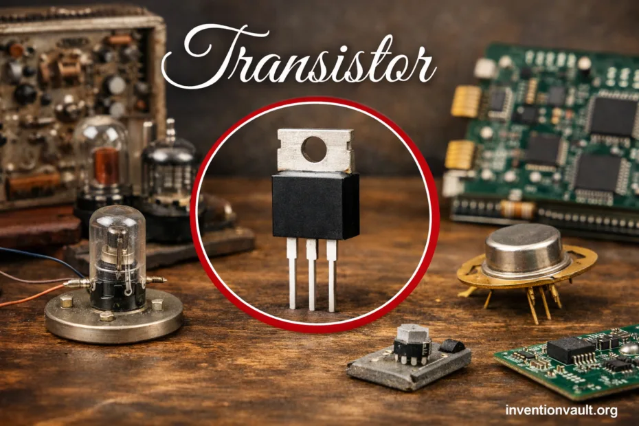
| Invention | Transistor (a solid-state electronic device) |
| Primary Purpose | Switching and amplifying electrical signals using semiconductor control |
| First Working Demonstration | December 16, 1947 (early point-contact transistor at Bell Labs) |
| Key Inventors | John Bardeen, Walter Brattain, William Shockley (core transistor invention era) |
| Organization | Bell Telephone Laboratories (Bell Labs) |
| Public Introduction | June 30, 1948 (widely cited public announcement) |
| Original Materials | Germanium was common early; silicon became dominant for stability and scaling |
| Physical Principle | Controlled conductivity in a semiconductor by shaping charge carriers (electrons/holes) with junctions or electric fields |
| Early Form | Point-contact first, then junction transistors that were more repeatable |
| Modern Workhorses | BJT (bipolar junction transistor) and MOSFET (metal–oxide–semiconductor field-effect transistor) |
| Major MOSFET Milestone | 1959 (key MOSFET development at Bell Labs; foundational for modern CMOS) |
| Why It Endures | Small, fast, efficient, and scalable from one device to billions on a single chip |
The transistor is the quiet engine behind modern electronics. It can act as a tiny switch or a signal booster, turning weak inputs into useful outputs. That single idea—controlling current with a small signal—made radios pocketable, computers practical, and sensors affordable.
- What a Transistor Does
- Why People Still Care
- How Transistors Work
- A Simple Picture in Words
- Major Transistor Families
- BJT
- MOSFET
- JFET
- IGBT
- Darlington Pair
- Phototransistor
- Key Moments in Transistor History
- From Single Devices to Integrated Circuits
- Scaling in Plain Numbers
- Where Transistors Show Up
- Common Specifications and What They Mean
- A Deeper Look at “Switch” and “Amplifier”
- Switching Mode
- Amplifier Mode
- Why the Transistor Was a Turning Point
- Transistor Terms You’ll See Often
- References Used for This Article
What a Transistor Does
- Switches power on and off with speed and precision.
- Amplifies signals so sound, radio, and data can travel cleanly.
- Shapes waveforms in analog circuits and logic circuits alike.
- Protects systems by handling power in controlled steps.
Why People Still Care
- Efficiency matters: a well-chosen MOSFET can waste very little energy.
- Scale matters: integrated circuits pack vast numbers of transistors in a small area.
- Reliability matters: solid-state devices last and behave consistently.
- Cost matters: mass production made electronics widely accessible.
How Transistors Work
A transistor is built from a semiconductor—most often silicon—whose conductivity can be tuned. Engineers do this by adding tiny amounts of other atoms, a process called doping. The result is a material that can carry current in a controlled way, not like a simple wire and not like an insulator.
Two common control styles dominate: junction control and field control. In a BJT, a small current into the base steers a larger current between emitter and collector. In a MOSFET, a voltage on the gate creates an electric field that opens or closes a channel between source and drain.
A Simple Picture in Words
- Input: a small signal you can control.
- Gate/Base: the “handle” that sets the device state.
- Output Path: a larger current that gets allowed, limited, or blocked.
- Result: amplification or switching with high repeatability.
Major Transistor Families
BJT
The bipolar junction transistor (BJT) uses both types of charge carriers, which helps it deliver strong gain and smooth analog behavior. Designers like BJTs in audio stages, sensor front-ends, and places where predictable amplification matters.
- Strength: high transconductance for clean amplification.
- Trade-off: needs base current, so control uses current drive.
- Common Forms: NPN and PNP.
MOSFET
The MOSFET is the main reason modern chips can hold so many devices. Its voltage-driven gate draws very little steady input current, and it can be made extremely small. You meet MOSFETs in CMOS logic, memory, and power conversion.
- Strength: excellent for fast switching and high-density integration.
- Key Metric: low RDS(on) for efficient power switching.
- Common Forms: n-channel and p-channel.
JFET
A junction FET (JFET) controls current with a reverse-biased junction. Many designs value its naturally low noise and gentle input behavior. It shows up in instrumentation, sensitive analog stages, and measurement circuits.
IGBT
The insulated-gate bipolar transistor (IGBT) blends MOSFET-style control with bipolar-style conduction. It shines in high-power switching where efficiency matters and voltages rise. You’ll find IGBTs in motor drives, industrial inverters, and other heavy-duty systems.
Darlington Pair
A Darlington pair combines two BJTs to behave like one device with much higher current gain. It’s popular when a small control signal must drive a larger load. The trade is extra voltage drop and slower switching in some cases.
Phototransistor
A phototransistor responds to light. Photons create charge carriers, and the device turns that into an electrical signal with built-in gain. It helps in optical sensors, interrupt switches, and simple light detection.
| Type | Control Style | Often Best for | Common Places You’ll See It |
|---|---|---|---|
| BJT | Current-driven base | Linear gain, low-distortion analog | Audio stages, sensor amplifiers, analog IC blocks |
| MOSFET | Voltage-driven gate field | Fast switching, dense integration | CPUs, memory, phone chips, power supplies |
| JFET | Junction pinch-off | Low noise, high input impedance | Precision analog front ends, measurement tools |
| IGBT | Gate-controlled bipolar conduction | High voltage and high power switching | Motor drives, industrial inverters, power modules |
Key Moments in Transistor History
- 1947: first working point-contact transistor demonstrated at Bell Labs.
- 1948: the term “transistor” becomes public; development accelerates in labs and industry.
- 1950s: junction transistors mature; silicon rises as a preferred material.
- 1954: early transistor radios show how portable electronics can be.
- 1956: Nobel Prize recognizes the transistor effect and its foundational impact.
- 1959: the MOSFET arrives, setting up CMOS as the future of digital logic.
- 1960s–1970s: integrated circuits scale rapidly; systems become smaller and more reliable.
- Today: microelectronics uses vast transistor counts for computing, sensing, and efficient power control.
From Single Devices to Integrated Circuits
Early circuits used discrete transistors soldered one by one. Integrated circuits changed that by building many transistors on one piece of silicon. Once you can manufacture devices together, you also connect them together with fine layers of metal. That’s the leap from “a transistor” to a whole system on a chip.
CMOS (complementary MOS) became a centerpiece because it can be extremely power-efficient in digital logic. In simple terms, CMOS pairs n-channel and p-channel MOSFETs so that, in steady states, very little current is wasted. This is one reason phones and laptops can be powerful without running hot all the time.
Scaling in Plain Numbers
| Integration Level | Typical Range | What It Feels Like |
|---|---|---|
| Discrete | 1 to a few transistors per function | Great for learning, repair, and specialized analog/power blocks |
| Small/Medium IC | Dozens to thousands | Classic building blocks: amplifiers, timers, simple logic |
| VLSI | Millions+ | Complex processors, graphics, and advanced communication chips |
| Modern SoC | Billions+ (varies by design) | Computing, memory, security, and radios in one silicon package |
Where Transistors Show Up
- Computing: CPUs and GPUs rely on dense MOSFET networks for logic and memory.
- Audio: amplifiers use BJTs or MOSFETs to turn small signals into speaker-driving power.
- Power Supplies: switching regulators use power MOSFETs for efficient conversion.
- Transportation Electronics: many control units use rugged transistors for sensing and power handling.
- Lighting: LED drivers use switching transistors for stable brightness and efficiency.
- Sensing: phototransistors and transistor-based sensor circuits convert tiny changes into readable signals.
Common Specifications and What They Mean
Datasheets can look intimidating, but most specs map to simple questions: How much can it handle, how fast does it switch, and how clean is the signal. Read them with that mindset and the numbers start to behave.
| Spec | Seen On | What It Tells You |
|---|---|---|
| VCE / VDS | BJT / MOSFET | The maximum voltage the device is designed to block in normal operation |
| IC / ID | BJT / MOSFET | The current it can carry within thermal limits |
| hFE (β) | BJT | Approximate current gain in certain regions (varies with conditions) |
| VTH | MOSFET | Gate threshold region where conduction begins (not the same as “fully on”) |
| RDS(on) | Power MOSFET | How much resistance remains when “on”; lower often means higher efficiency |
| Leakage | Many types | Small off-state current; relevant for power and battery designs |
| fT / Switching Times | BJT / MOSFET | Speed limits; impacts radio-frequency work and fast digital switching |
| Package | All | Heat handling and mounting style; packaging shapes real-world performance |
A Deeper Look at “Switch” and “Amplifier”
Switching Mode
In switching, a transistor spends most of its time either off (blocking current) or on (conducting with low loss). That’s why power electronics loves the MOSFET. When engineered well, it wastes little energy as heat.
- Goal: minimize loss and heat.
- Focus: RDS(on), switching speed, thermal design.
Amplifier Mode
In amplification, the device sits in a controlled region where small changes at the input cause smooth changes at the output. Here, a BJT can feel natural because it offers strong linearity in many analog designs. A careful bias point keeps signals clean.
- Goal: accurate signal shape.
- Focus: gain, noise, distortion, stability.
Why the Transistor Was a Turning Point
Before the transistor era, many electronic systems relied on vacuum tubes—large, power-hungry parts that generated significant heat. The transistor offered a path to miniaturization and efficiency without sacrificing functionality. This shift made it realistic to put sophisticated electronics into everyday life.
It also reshaped manufacturing. Once silicon processing matured, transistors could be produced with extraordinary consistency. That reliability is why semiconducter technology became the backbone of global electronics supply chains—chips can be designed, tested, and replicated at scale with predictable results.
Transistor Terms You’ll See Often
- Junction: the boundary between differently doped regions that guides carrier flow.
- Bias: the steady voltages/currents that place a transistor in the desired operating region.
- Saturation: a switching “fully on” state for many BJTs, used for digital or power control.
- Cutoff: a switching “off” state where the device blocks current as much as practical.
- Body Diode: a built-in diode effect common in power MOSFET structures; relevant in many power paths.
- Thermal Limits: real performance depends on heat removal, not just electrical ratings.
References Used for This Article
- University of Central Florida (Pressbooks) — Semiconductors and Doping – University Physics Volume 3: A clear overview of how doping creates n-type and p-type semiconductors and changes conductivity.
- The Nobel Prize — The Nobel Prize in Physics 1956 (Summary): Confirms the award and citation recognizing the discovery of the transistor effect.
- Computer History Museum — Invention of the Point-Contact Transistor: Documents the earliest successful point-contact transistor work in late 1947 and its technical significance.
- Computer History Museum — Metal Oxide Semiconductor (MOS) Transistor Demonstrated: Summarizes the 1959 Bell Labs MOS transistor milestone and why it enabled modern CMOS scaling.
- IEEE Electron Devices Society — 75th Anniversary of the Transistor: Provides an IEEE-published historical framing of the transistor’s invention and its foundational impact on electronics.
- National Institute of Standards and Technology (NIST) — John Bardeen and Transistor Physics (PDF): Offers a NIST-hosted historical and technical perspective on Bardeen’s role in transistor research.
- Georgia State University (HyperPhysics) — Doped Semiconductors: Explains how dopants change carrier populations and why that matters for semiconductor devices.